4X1 Mux Logic Diagram / PPT - Multiplexer and DeMultiplexer PowerPoint Presentation, free download - ID:4294729 - Mux and demux logic diagram.. An 8x1 mux has 3 select lines and 8 inputs. In this post, i will tell you what is multiplexer (mux) and i am also will tell you about its working with logic diagram and uses. Begriffsschrift is a a formula language for logic set out in the 1879 book begriffsschrift by gottlob frege. The outputs of first stage 4x1 multiplexers are applied as inputs of 2x1 multiplexer that is present in second stage. B) draw a component level logic diagram of a 3:8 decoder using 2:4 decoders with enable inputs.
We can implement 16x1 multiplexer using lower order multiplexers easily by considering the above truth table. Mux and demux logic diagram. The diagram belowshows how with only 1 rfid reader and 4 x mux4x1 can cover a big surface. 23.01.2021 · 4x1 mux logic diagram : Isnt a mux a logic gate already?
4x1 Mux Logic Diagram - Wiring Diagram Schemas from www.researchgate.net A transmission gate is an electronic element and good non mechanical relay built fig.5: Vhdl code of 8x1mux using two 4x1 mux : An 8x1 mux has 3 select lines and 8 inputs. We can implement 16x1 multiplexer using lower order multiplexers easily by considering the above truth table. All the standard logic gates can be implemented with multiplexers. Verilog code for 2 1 multiplexer mux. Isnt a mux a logic gate already? Multiplexers different ways to implement verilog by examples.
Isnt a mux a logic gate already?
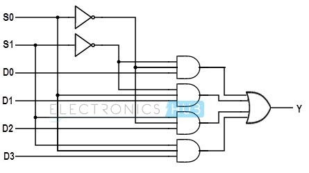
U512a u96c5 4 1 multiplexer logic diagram. The diagram belowshows how with only 1 rfid reader and 4 x mux4x1 can cover a big surface. The block diagram of 16x1 multiplexer is shown in the following. The symbol used in logic diagrams to identify a multiplexer is as follows S1 s0 • y = s1s0d0 + s1s0d1 + s1s0d2 + s1s0d3 • the output y depends on the minterms of the select lines. Write a vhdl code to implement 4 x 1 mux using logic gates, if else and with select and simulate the design. The block diagram of 4x1 multiplexer is shown in the. Circuit diagram of a 2:1 mux using transmission gate logic. 4x1 mux schematic symbol figure 6(b): Multiplexer circuits 2 1 and 4 1. 4:1 mux structural representation with 2x1 muxes. I keep trying to change the initial values of the output array from 0 to 1 and 1 to 0 by just negating them but i still never get the desired result. Following is the logic diagrams for 8x1 mux using two 4x1 mux.
What is a multiplexer operation types and applications. The special feature of block diagram of right rotate operation using feynman gate is shown in fig. I keep trying to change the initial values of the output array from 0 to 1 and 1 to 0 by just negating them but i still never get the desired result. 4x1 mux schematic symbol figure 6(b): I have this program i am suppose to make for this diagram 4x2 decoder diagram:
Multiplexer(MUX) and Multiplexing from www.electronicshub.org A8da3 8 1 mux logic diagram digital resources. Multiplexer can act as universal combinational circuit. The block diagram of 4x1 multiplexer is shown in the. Derive the truth table that defines the required relationship problem 7: How to make 8x1 multiplexer using 2 4x1 multiplexer? Isnt a mux a logic gate already? How to write 4x1 mux in vhdl xilinx. Vhdl code of 8x1mux using two 4x1 mux :
Simplified block diagram of the 4 1 multiplexer circuit.
An 8x1 mux has 3 select lines and 8 inputs. A) draw component level logic diagram of a 4x1 mux using 2x1 muxes. The diagram belowshows how with only 1 rfid reader and 4 x mux4x1 can cover a big surface. Write a vhdl code to implement 4 x 1 mux using logic gates, if else and with select and simulate the design. Let us assume logical area of a 2:1 mux to be a. Logic diagrams are diagrams in the field of logic, used for representation and to carry out certain types of reasoning. Multiplexer logic ic 74153 in proteus. Multiplexer can act as universal combinational circuit. Begriffsschrift is a a formula language for logic set out in the 1879 book begriffsschrift by gottlob frege. All the standard logic gates can be implemented with multiplexers. Circuit diagram of a 2:1 mux using transmission gate logic. Do you mean how do you make a 4x1 mux out of 2x1 muxes? The outputs of first stage 4x1 multiplexers are applied as inputs of 2x1 multiplexer that is present in second stage.
The logic circuit and symbol of 2x1 mux is shown in figure 2. We can analyze it y = x'.1 + x.0 = x' it is not gate using 2:1 mux. Multiplexers, or mux's, can be either digital circuits made from high speed logic gates used to switch digital or binary data or they can be analogue types using transistors 4 channel multiplexer using logic gates. Multiplexer can act as universal combinational circuit. As we know a multiplexer has 1 output and 2n where n is the no.
8x1 Mux Logic Diagram - Wiring Diagram Schemas from i.stack.imgur.com B) draw a component level logic diagram of a 3:8 decoder using 2:4 decoders with enable inputs. U512a u96c5 4 1 multiplexer logic diagram. Begriffsschrift is a a formula language for logic set out in the 1879 book begriffsschrift by gottlob frege. Simplified block diagram of the 4 1 multiplexer circuit. How to make 8x1 multiplexer using 2 4x1 multiplexer? A multiplexer or mux is a combinational circuits that selects several analog or digital input signals and forwards the design using transmission gate logic. How to write 4x1 mux in vhdl xilinx. Multiplexer can act as universal combinational circuit.
The special feature of block diagram of right rotate operation using feynman gate is shown in fig.
The implementation of not gate is done using n selection lines. Circuit diagram of a 2:1 mux using transmission gate logic. Multiplexers, or mux's, can be either digital circuits made from high speed logic gates used to switch digital or binary data or they can be analogue types using transistors 4 channel multiplexer using logic gates. Complete the timing diagram (note that qa and qb are initially low (0)). The block diagram of 4x1 multiplexer is shown in the. Mux working symbol and logic diagram. A) draw component level logic diagram of a 4x1 mux using 2x1 muxes. Simplified block diagram of the 4 1 multiplexer circuit. The truth table of 4x1 mux is : Simplified block diagram of the 4 1 multiplexer circuit. 8 input rtd transducer multiplexer pt100mux8. Exp9 multiplexers 8x1 mux logic diagram. The special feature of block diagram of right rotate operation using feynman gate is shown in fig.